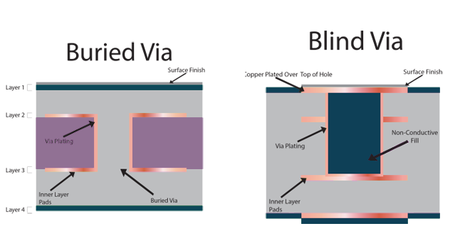
Blind & Buried Via

When PCB space is limited, or you're working with tight plated through hole constraints, Blind and Buried Vias may be the answer. Blind & Buried Via technology has played a pivotal role in squeezing more capability into a smaller space. By shortening vias to only pass through necessary layers, more surface area become available for components.
Key benefits include:
- Ability to meet the density constraints of lines and pads on a typical design without increasing the layer count or board size
- PCB aspect ratio reduction
Blind Via is a copper plated hole that connects only one outer layer to one or more inner layers. A blind via never goes all the way through a circuit board. In terms of design, blind vias are defined in a separate drill file.
